RING_OF_DOOM.sh
TIME FRAME: April 2023
LED Ring for the Mate ROV 2023-2023 Competition
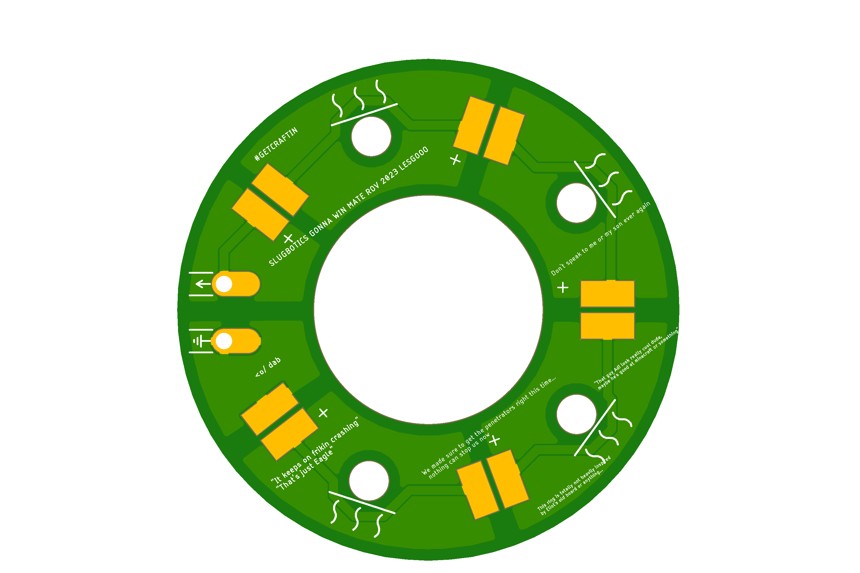
0|COOL PICTURE
1|CONTEXT
This project earned a spot here because, while the design may not seem to be extremely complicated nor unique at first glance, designing this ring taught me much of the fundamental concepts in the PCB design process I still heavily rely on and use to this day. It is one of the more impactful projects towards my self growth I have been given the opportunity to work on.
This board was done when Slugbotics (A vibrant and geeky robotics club at UCSC... more info on that on my resume!), had only 3 subteams for the ROV competition. One of the responsibilities for the electrical department involved finding solutions to any requirement for the vehicle that dealt with power management or the boards themselves. Issues pertaining to visibility underwater for our camera systems was a major focus for our team.
I picked up EDA software 5 months before this specific project, so despite feeling green in various areas, I felt confident enough to tackle the board for the actual light fixture on my own. Despite this confidence, I made it a point to thoroughly understand and even borrow concepts from light systems used in previous years and in other projects to optimize the design. There was a lot to learn from past successes and failures, and continuous improvement can’t happen unless you fully understand the baseline first.
Let's get into the design.
2|DESIGN
- There were a few main ideas to consider when designing this board:
- The camera needed to be provided with enough light to veiw the ROV's surroundings.
- Power efficiency is paramount, as the 48V PSU needs to supply power for other crucial systems as well.
- The light will be housed in a small airtight enclosure. That means heat is a major point of consideration.
Given the light requirements and the important emphasis on efficiency, the obvious move here is the best one: to focus on sourcing high power LED diodes. Development for this component has reached a point where very powerful LEDs capable of illuminate vast distances are not only perfect for our circumstances, but also accessible. Being energy efficient and very capable while still also remaining rather cheap, purchasing these diodes and slapping them on a board was the clear way to go.
However, finding the right components that play well with the constraints and situation given wasn’t as intuitive. Thankfully, Digikey had some really good-performing LEDs already stocked at reasonable prices. Taking max current draw and voltage requirements in mind, I ended up purchasing a batch of J-Series 2138-JR5050AWT-Q diodes.
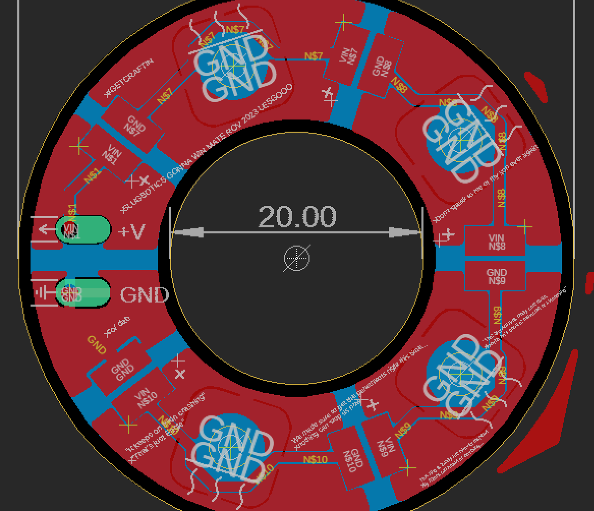
They had a current max of 1A with a minimum operating 5.8V requirement, so it fit extremely well into the constraints I needed to consider. Heat dissipation became the next focus. I ended up turning to previous designs of similar tasks in my club as well as online resources. Despite taking an embarrassing 5 months, this was when I finally discovered a Holy Grail treasured by all PCB designers: The Ground Plane.
(Needless to say, ground planes have since become a fundamental backbone of most of my projects.)
There is a good chance those with an EE background in the industry already know about what they do. However, for the sake of the story and for those curious, I decided that a quick blurb about them couldnt hurt. Feel free to skip the next section if you are here only for the project!
2A| ~/DESIGN/GROUND_PLANES
Simply put, ground planes are large areas of copper on a PCB that serve as a common ground for all electrical components in its area. This provides designers the luxury of making better routes and traces for their PCB, as the space requirement for possible ground lines are gone.
Ground planes don’t only serve as a quality of life benefit for designers though. In fact, it is a critical component that plays a larger role in the real world beyond what one might assume at first.
- Signal Integrity-
- Power Distribution-
- Heat Dissipation-
They are essential for:
- Test
- idk
F1: EAGLE Footprint Editor
3| ANALYSIS
- [cd ..] BACK TO HOME